

Welcome to Panamint
About Us
Our company creates electronics using ecological materials and processes wherever possible. We are committed to revolutionizing the electronics industry. Printing with nanomaterials when manufacturing products such as batteries or LCD displays is the future that brings a wealth of new possibilities.
Meet our team!

Team
Panamint was founded in 2020 by experts and enthusiasts with many years of experience in nanotechnology, semiconductor fabrication, embedded systems, industrial machine learning, chemistry, and product design. We are driven by an appreciation for the natural world, our place in it, and the elusive art of simplicity.

CEO, holds a PhD degree in physics from the University of Pennsylvania, Philadelphia, USA, where he studied complex fluids and networks of carbon nanotubes. Previously the CTO of Zikon Inc., a nanotechnology company that developed unique electronic paper display technology. He has over 25 years of experience in nanotechnology, semiconductor manufacturing, as well as MEMS and Deep tech startups. Mateusz Bryning has consulted on many projects relating to micro and nano technologies, including inventions, prototyping, IP, and technological strategy.

CTO, previously the CTO of GamerHash, is a graduate of the University of Silesia, Katowice, Poland. He holds a PhD degree in physics, with a specialization in correlated electronic systems. Lech Kalinowski has over 10 years of experience in condensed matter physics, printing technologies, and data science. He has excellent knowledge of conducting basic research in the physics of quantum materials.

COO, co-founder and investor in Panamint, CEO at the Nanonet Foundation. A graduate of the University of Münster, Münster, Germany, he holds a PhD degree in nanotechnology with a specialism in electroluminescence. For 15 years, he has specialized in advanced EU research projects.

Principal Designer, a graduate of the Silesian University of Technology, Gliwice, Poland. He holds a master’s degree in interior and industrial design. He has over 16 years of experience in industrial, interior and product design, and also boasts extensive knowledge of packaging design and presentation of POS and display end products.

Lead Chemist, a graduate of the Silesian University of Technology, Gliwice, Poland. She holds an MSc in chemical technology. She specializes in organic synthesis and spectroscopic methods. She has two years of experience in formulating emulsions and dispersions for household, cosmetic and technical chemistry.

She holds the position of Management Assistant. In 2023 graduated with honors and received a master's degree in English Philology at the University of Silesia in Katowice, Poland. Over the years she has gained experience in translating spoken and written English. Specializes in the translation of legal and administrative writings.

Works as a Junior Programmer, currently a 3rd year student of Micro&Nanotechnology engineering degree at the University of Silesia in Katowice, Poland. Takes special interest in programming languages such as Python, C++ and Dart.

Junior Programmer at Panamint. Similarly to Lana, she is currently in the process of getting engineering degree in the field of Micro&Nanotechnology at the University of Silesia in Katowice, Poland. Interested mostly in Product Development.
Mission
"Simplicity is the ultimate sophistication" - Leonardo da Vinci
Our goal is to simplify the design and manufacture of embedded electronics systems to create solutions tailored to your specific needs. Sustainable manufacturing is key to this approach. By using ecological materials and processes wherever possible, and focusing on robust and resilient technologies that are “just right” for their purpose, we reduce e-waste and the environmental impact of electronics manufacturing. Thanks to advances in functional nanomaterials and printed electronics, we effectively achieve performance targets that previously required costly, wasteful, and environmentally harmful processes, materials, and tools.
Today’s over-engineered metal, plastic, and epoxy packaging is responsible for much of the generated e-waste. Our company favors minimalist packaging made from ecological and biodegradable materials. We dynamically adapt modern technologies to the constantly changing needs of consumers, driving innovation to meet the needs of tomorrow. By integrating printing processes of multiple components into whole printed systems, we lower manufacturing costs, improve yields and lessen the environmental impact of our products while simultaneously creating value by reaching higher on the value chain.
Projects
One of the problems facing the industry today is traceability and product safety. We care about the right conditions for the storage of perishable products, in which the storage time and temperature of open packaging play a particularly important role. We want to know what is happening with the product from its inception to its final stage – disposal.
Traditional solutions are too expensive and create too much hazardous waste.
Our solution alleviates both of these problems.
Smart Labels
Western Europe’s smart labels market is expected to become a US$ 4.0 BN industry by 2030. The global smart labels market is forecasted to register a dexterous CAGR of ~13%, expanding more than threefold across the 2020–2030 forecasted period.
The challenge we face is:
- Proper storage conditions for perishable products
- Storage times of open packaging
- Storage temperature
- Product authentication
- Supply Chain Logistics
- Consumers’ right to know about the correct use and disposal of products
- Traditional solutions based on ordinary electronics are too expensive and consequently create a lot of hazardous waste

Our solution
Printed e-labels for transport and storage monitoring enabled by PANAMINT printed electronics
- Low costs with minimal waste
- Meeting sustainability, regulatory, performance, and quality goals throughout the product life cycle
- Integration with existing logistics systems
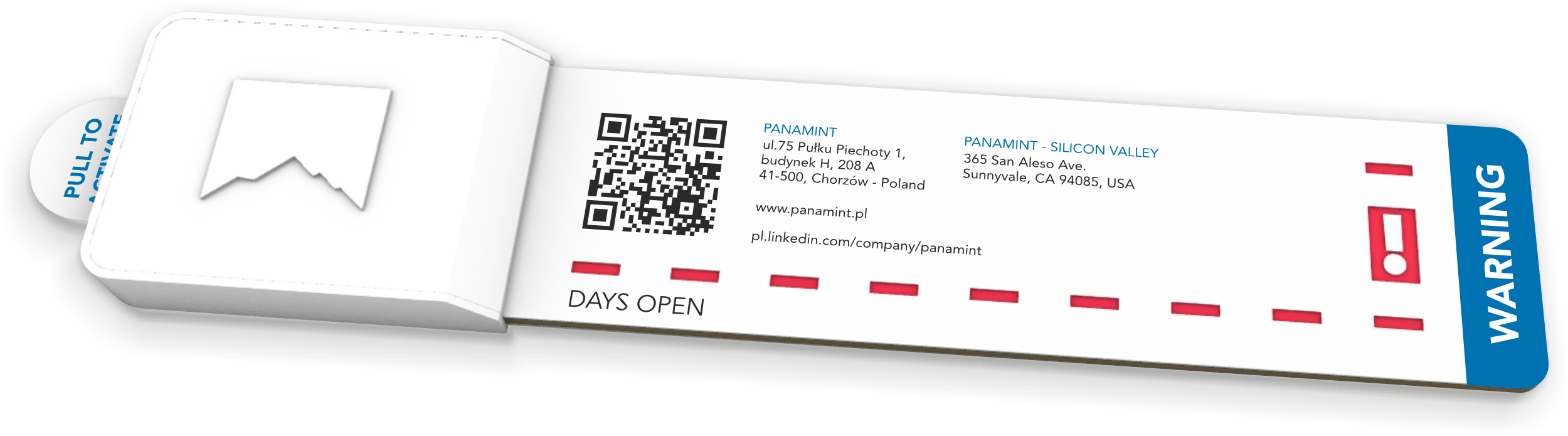
Smart Labels
in the food industry
– a better way for origin tracking, product safety and proper storage
We currently waste billions of tons of food every year. Smart labels will reduce this by keeping track of the freshness of a given product and ensuring the visibility of this information for consumers. Both ordinary consumers and the entire food and logistics industry will be able to use this information to measure product freshness as it travels down the supply chain.
This information will help identify where the inefficiencies causing spoilage are occurring and what can be done to optimize these processes. Consequently, we will contribute to a considerable reduction of the industry’s negative environmental impact.
The benefits of intelligent labeling in the food industry